News
Feb. 24, 2025
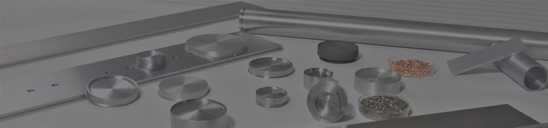
Sputtering silicon is a process where a thin film of silicon is deposited onto a substrate by bombarding a solid silicon target with energetic ions, typically from an inert gas like argon, causing the silicon atoms to be ejected from the target and condense onto the substrate, creating a thin silicon film; essentially, it's a physical vapor deposition (PVD) technique used to precisely deposit silicon layers on various materials within a vacuum chamber.

The sputtering process is a critical technique in thin-film deposition, widely used in semiconductors, optics, solar panels, and protective coatings. As a leading method for high-precision coatings, sputtering ensures uniform film deposition on various substrates. Understanding the step-by-step process helps manufacturers optimize efficiency, improve product quality, and meet industry standards. This article explores the key stages of sputtering from a manufacturer’s perspective and highlights its significance in modern technology.
The global sputtering target market is expected to grow to $5.6 billion by 2027, driven by increasing demand in electronics, aerospace, and energy sectors (MarketsandMarkets). With advancements in nanotechnology and semiconductor fabrication, sputtering remains a preferred coating method due to its high uniformity, adhesion strength, and versatility.
1. Preparation of the Vacuum Chamber
The process begins with evacuating the chamber to create a low-pressure environment.
This prevents contamination and allows precise control over plasma formation.
Typical pressure: 1×10⁻³ to 1×10⁻⁶ Torr.
2. Insertion of the Sputtering Target and Substrate
A high-purity sputtering target (metal, alloy, or ceramic) is placed in the chamber.
The substrate, which will receive the thin-film coating, is positioned opposite the target.
Targets are chosen based on application requirements such as conductivity, reflectivity, and durability.
3. Plasma Generation and Ion Bombardment
A working gas (typically Argon, Ar) is introduced into the vacuum chamber.
A high-voltage electric field ionizes the gas, creating a plasma.
Positive ions accelerate towards the sputtering target, striking its surface with high kinetic energy.
4. Ejection of Target Material (Sputtering Effect)
The ion bombardment knocks off atoms from the target material.
These ejected atoms move toward the substrate in a controlled trajectory.
The sputtering yield depends on ion energy, target composition, and chamber pressure.
5. Thin-Film Deposition on the Substrate
The sputtered atoms condense and form a uniform thin-film layer on the substrate.
Film thickness is controlled through sputtering duration, power input, and deposition rate.
The resulting film properties (electrical, optical, or mechanical) depend on target material selection and process parameters.
6. Post-Deposition Annealing and Quality Control
After deposition, the thin film may undergo annealing to enhance crystallinity and adhesion.
Quality control techniques such as X-ray diffraction (XRD), Scanning Electron Microscopy (SEM), and profilometry verify the film's thickness, uniformity, and composition.
Manufacturers follow industry standards like ISO 9001 and ASTM to ensure reliability.
1. DC Sputtering
Used for conductive materials such as metals.
Simple setup with constant direct current (DC) power.
Common in semiconductor and industrial coatings.
2. RF Sputtering
Used for dielectric and insulating materials.
Employs radio frequency (RF) power to sustain plasma.
Essential for depositing ceramic and complex oxide films.
3. Magnetron Sputtering
Involves magnetic fields to increase ionization efficiency.
Provides higher deposition rates and improved film quality.
Ideal for large-scale production in electronics and optics.
4. Reactive Sputtering
Introduces reactive gases (e.g., Oxygen, Nitrogen) into the chamber.
Forms compound films such as TiN, Al₂O₃, or SiO₂.
Used for hard coatings, optical layers, and protective films.
High Uniformity: Achieves consistent thin-film thickness across large areas.
Excellent Adhesion: Strong bonding between the film and substrate.
Versatile Material Compatibility: Deposits metals, alloys, ceramics, and composite materials.
Environmentally Friendly: No need for hazardous chemical precursors.
Scalability: Used in mass production of semiconductors, display panels, and precision coatings.
With rapid advancements in AI-driven automation, nanotechnology, and flexible electronics, sputtering technology is evolving to meet new industrial challenges:
Atomic Layer Sputtering (ALS) for ultra-thin films with atomic precision.
In-situ monitoring with AI-driven process control for real-time quality assurance.
Eco-friendly sputtering to minimize material waste and energy consumption.
Increased adoption in 5G and quantum computing for high-performance microelectronics.
The sputtering process is an essential technology for manufacturing high-performance thin films across diverse industries. Understanding its step-by-step methodology, key techniques, and material selection enables manufacturers to optimize production efficiency, film quality, and application performance.
For businesses looking to enhance their thin-film deposition processes, investing in advanced sputtering technology ensures higher yield, cost-effectiveness, and compliance with global standards. As electronics, optics, and energy sectors continue to expand, sputtering remains a cornerstone of next-generation material science.
Previous
NoneNext
Remarkable Benefits of Titanium-Silicon Sputtering TargetsRELATED PRODUCTS
Premium Chromium Sputtering Targets for corrosion-resistant PVD coatings. 99.5%-99.95% purity, HIP/HP technology, customizable solutions. Ideal for automotive, photovoltaic, and decorative industries. Trusted quality with ISO-certified production.
Our titanium-aluminum(TiAl) targets are used for decorative coatings on electronic devices. In addition, thanks to the resistance to oxidation and toughness, our titanium-aluminum targets are also widely used as the coatings of milling machines, drills and other tools.
Thanks to the toughness, high thermal stability and resistance to oxidation, our chromium-aluminum (CrAl) targets are widely used as the coatings of milling machines, drills and other tools.
RELATED NEWS
Jun. 20, 2024
PVD – acronym for Physical Vapor Deposition – is an environmental friendly high vacuum coating technology for thin film deposition on different kinds of base materials in plasma atmosphere.
Jun. 20, 2024
PVD Thin Film Coating for Hardware Tool and Mould
Protective wear coatings can be used for sheet metal pressing, steel forming, aluminum foundries, and for the production of machine parts and components for the automotive industry.
Jun. 20, 2024
Sputtering as a phenomenon was first observed back in the 1850s but remained a scientific curiosity until the 1940s, when diode sputtering was firstly used to some significant extent as a commercial coating process.


