News
Feb. 24, 2025
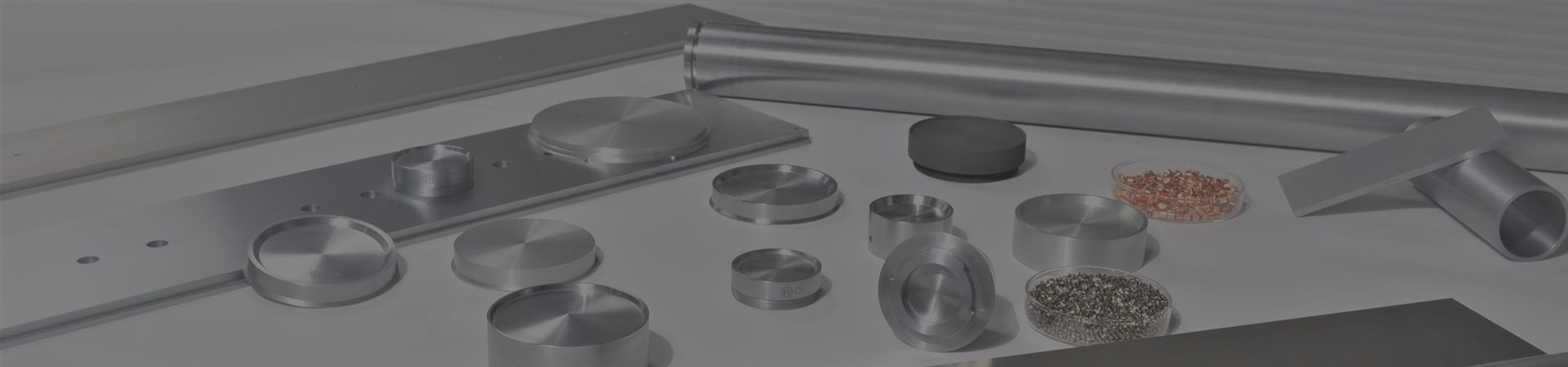
In the ever-evolving world of thin-film deposition, Titanium-Silicon (Ti-Si) sputtering targets have emerged as a critical material for industries such as semiconductors, optics, and protective coatings. These advanced targets offer a unique combination of properties that enhance film performance, making them highly sought after in high-tech applications. As a manufacturer or procurement specialist, understanding the benefits, applications, and industry significance of Ti-Si sputtering targets is crucial for making informed sourcing decisions.

The global sputtering target market is projected to reach $5.6 billion by 2027, driven by increasing demand in electronics, aerospace, and energy sectors (MarketsandMarkets). Titanium-Silicon sputtering targets are particularly valuable due to their ability to produce thin films with enhanced durability, oxidation resistance, and high-performance electrical properties.
1. Superior Hardness and Wear Resistance
Titanium-Silicon films are widely used in protective coatings due to their exceptional hardness. These coatings significantly extend the lifespan of industrial tools, cutting instruments, and high-performance components by reducing wear and friction.
2. Excellent Oxidation and Corrosion Resistance
Industries such as aerospace and electronics require materials that withstand extreme environmental conditions. Ti-Si sputtering targets produce films that exhibit outstanding oxidation and high-temperature resistance, making them ideal for applications exposed to harsh conditions.
3. High Thermal Stability for Advanced Applications
The high melting point and thermal stability of Titanium-Silicon coatings allow them to perform exceptionally well in high-temperature environments. This property is crucial for semiconductor manufacturing and optical applications where thermal degradation can be a significant issue.
4. Improved Electrical Conductivity and Performance
Titanium-Silicon films enhance electronic device performance by offering a stable and conductive surface. These films are widely used in the production of thin-film transistors (TFTs), touch panels, and microelectronic circuits.
5. High Adhesion and Uniform Film Deposition
One of the critical aspects of thin-film coating is achieving a uniform and adherent layer. Ti-Si sputtering targets ensure precise film thickness and excellent adhesion to various substrates, which is essential for applications requiring reliability and consistency.
1. Semiconductor and Microelectronics
Used in integrated circuits (ICs) and microelectromechanical systems (MEMS)
Essential for thin-film transistors (TFTs) in display technologies
Provides electromagnetic interference (EMI) shielding
2. Optics and Photonics
Titanium-Silicon coatings are utilized in anti-reflective coatings for optical lenses and cameras
Used in laser mirrors and beam splitters
3. Protective Coatings for Aerospace and Automotive Industries
Enhances the durability of engine components and aircraft coatings
Used in wear-resistant coatings for high-stress automotive parts
4. Renewable Energy and Solar Cells
Applied in thin-film solar panels to improve efficiency and longevity
Utilized in hydrogen storage materials due to its superior stability
To ensure high performance, Titanium-Silicon sputtering targets must meet stringent industry standards. Manufacturers should comply with:
ISO 9001 & ISO 14001 for quality and environmental management
ASTM specifications for material purity and composition consistency
SEM and X-ray diffraction (XRD) analysis for microstructure verification
Additionally, customization options such as different purity levels, diameters, and thicknesses allow manufacturers to tailor sputtering targets to specific industrial needs.
With continuous advancements in material science, the demand for high-performance coatings is expected to grow. Future developments include:
Nano-engineered Titanium-Silicon films for improved mechanical and electrical properties
Sustainable production techniques to minimize waste and environmental impact
Increased adoption in flexible electronics and next-generation semiconductor devices
Titanium-Silicon sputtering targets are a vital material in modern thin-film technology, offering superior hardness, oxidation resistance, and excellent electrical conductivity. Their applications in semiconductors, optics, aerospace, and renewable energy make them a valuable investment for manufacturers and procurement professionals.
For businesses looking to enhance their thin-film deposition processes, sourcing high-quality Titanium-Silicon sputtering targets from a reputable manufacturer ensures reliability, efficiency, and compliance with industry standards. As the market for advanced coatings and semiconductor materials expands, investing in high-performance sputtering targets will be key to staying competitive in the evolving electronics and industrial sectors.

RELATED PRODUCTS
Premium Chromium Sputtering Targets for corrosion-resistant PVD coatings. 99.5%-99.95% purity, HIP/HP technology, customizable solutions. Ideal for automotive, photovoltaic, and decorative industries. Trusted quality with ISO-certified production.
Our titanium-aluminum(TiAl) targets are used for decorative coatings on electronic devices. In addition, thanks to the resistance to oxidation and toughness, our titanium-aluminum targets are also widely used as the coatings of milling machines, drills and other tools.
Thanks to the toughness, high thermal stability and resistance to oxidation, our chromium-aluminum (CrAl) targets are widely used as the coatings of milling machines, drills and other tools.
RELATED NEWS
Jun. 20, 2024
PVD – acronym for Physical Vapor Deposition – is an environmental friendly high vacuum coating technology for thin film deposition on different kinds of base materials in plasma atmosphere.
Jun. 20, 2024
PVD Thin Film Coating for Hardware Tool and Mould
Protective wear coatings can be used for sheet metal pressing, steel forming, aluminum foundries, and for the production of machine parts and components for the automotive industry.
Jun. 20, 2024
Sputtering as a phenomenon was first observed back in the 1850s but remained a scientific curiosity until the 1940s, when diode sputtering was firstly used to some significant extent as a commercial coating process.


